Adp200er Schematic Exclusive - |best|
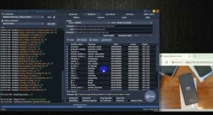
This public link is valid for 7 days and shares a thread, including any personal information you added. This link or copies made by others cannot be deleted. If you share with third parties, their policies apply. Can’t copy the link right now. Try again later.
Pin 7 of U1 is not ground. It is a -5V reference rail. Using a standard TL494 datasheet will mislead your repair.
Uses a MOSFET and a controller to maintain a stable, high DC voltage. Common components include the PFC MOSFET and diode 1.2.2 . Standby Converter: Generates the 5Vsb5 cap V sub s b end-sub using a specialized IC. B. Secondary Side (Cold)
: Large radial electrolytic capacitors (such as 400V 470uF) are often used in the high-voltage section and can degrade over time. Risk Warning : Do not attempt to use an adp200er schematic exclusive
Driven by a specialized PFC controller IC, this stage forces the input current to follow the input voltage waveform.
: A push-pull converter stage (often utilizing the DDA001AG or DNP012AH ICs) that delivers +12V (16A) when the console is fully powered. Functional Schematics and Community Guides
When the power button is pressed, the motherboard drops a active-high return signal ( PS_ON / SYS_DET ) back into the power supply. This public link is valid for 7 days
When the user presses the console power button, the motherboard returns a high signal ( PS_ON ) to the power supply. This wakes up the heavy-duty power delivery architecture.
The only route forward is the path of collective experience. Through sharing findings on platforms like EEVblog, Badcaps, and specialized forums, individuals have managed to create a "people's schematic"—a functional, if fragmented, understanding of the ADP-200ER's operations. Whether you are a professional technician or a DIY hobbyist, if you find yourself troubleshooting this unit, you are stepping into a world where the official map is hidden. Your success will depend on your own skills and the aggregated wisdom of the community that has come before you.
A user on the monitor.net.ru forum provided a detailed case study of trying to repair an ADP-200ER where the main MOSFET kept failing. This real-world example perfectly illustrates the challenges of working without a schematic. Can’t copy the link right now
4-Pin Logic Connector (Standby/Control) + Dual Blade Terminals (+12V) Architectural Breakdown of the Schematic
Features a 4-pin small connector to the motherboard. Functional Block Diagram


Post Comment